Future electronic components to be printed like newspapers
A new manufacturing technique uses a process similar to newspaper printing to form smoother and more flexible metals for making ultrafast electronic devices.
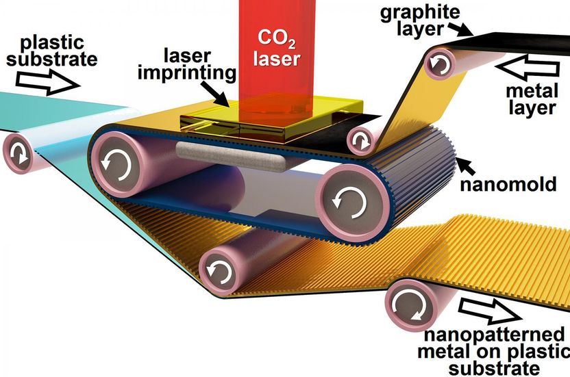
Roll-to-roll laser-induced superplasticity, a new fabrication method, prints metals at the nanoscale needed for making electronic devices ultrafast.
Purdue University image/Ramses Martinez
The low-cost process, developed by Purdue University researchers, combines tools already used in industry for manufacturing metals on a large scale, but uses the speed and precision of roll-to-roll newspaper printing to remove a couple of fabrication barriers in making electronics faster than they are today.
Cellphones, laptops, tablets, and many other electronics rely on their internal metallic circuits to process information at high speed. Current metal fabrication techniques tend to make these circuits by getting a thin rain of liquid metal drops to pass through a stencil mask in the shape of a circuit, kind of like spraying graffiti on walls.
"Unfortunately, this fabrication technique generates metallic circuits with rough surfaces, causing our electronic devices to heat up and drain their batteries faster," said Ramses Martinez, assistant professor of industrial engineering and biomedical engineering.
Future ultrafast devices also will require much smaller metal components, which calls for a higher resolution to make them at these nanoscale sizes.
"Forming metals with increasingly smaller shapes requires molds with higher and higher definition, until you reach the nanoscale size," Martinez said. "Adding the latest advances in nanotechnology requires us to pattern metals in sizes that are even smaller than the grains they are made of. It's like making a sand castle smaller than a grain of sand."
This so-called "formability limit" hampers the ability to manufacture materials with nanoscale resolution at high speed.
Purdue researchers have addressed both of these issues - roughness and low resolution - with a new large-scale fabrication method that enables the forming of smooth metallic circuits at the nanoscale using conventional carbon dioxide lasers, which are already common for industrial cutting and engraving.
"Printing tiny metal components like newspapers makes them much smoother. This allows an electric current to travel better with less risk of overheating," Martinez said.
The fabrication method, called roll-to-roll laser-induced superplasticity, uses a rolling stamp like the ones used to print newspapers at high speed. The technique can induce, for a brief period of time, "superelastic" behavior to different metals by applying high-energy laser shots, which enables the metal to flow into the nanoscale features of the rolling stamp - circumventing the formability limit.
"In the future, the roll-to-roll fabrication of devices using our technique could enable the creation of touch screens covered with nanostructures capable of interacting with light and generating 3D images, as well as the cost-effective fabrication of more sensitive biosensors," Martinez said.
Original publication
Other news from the department science
These products might interest you
Octet R2 / Octet R4 / Octet R8 by Sartorius
Full power on 2, 4 or 8 channels: Label-free and GxP-compliant analysis of molecular interactions
Innovative label-free real-time protein quantification, binding kinetics and rapid screenings
Octet RH16 and RH96 by Sartorius
Efficient protein analysis for process optimisation and manufacturing control in high-throughput
Label-free protein quantification and characterization of protein-protein interactions

Octet SF3 by Sartorius
Surface Plasmon Resonance (SPR) using Single Dynamic Injections for Kinetics and Affinities
Curvature is Key - Adding a ‘Third Dimension’ to the Binding Curve

Get the life science industry in your inbox
By submitting this form you agree that LUMITOS AG will send you the newsletter(s) selected above by email. Your data will not be passed on to third parties. Your data will be stored and processed in accordance with our data protection regulations. LUMITOS may contact you by email for the purpose of advertising or market and opinion surveys. You can revoke your consent at any time without giving reasons to LUMITOS AG, Ernst-Augustin-Str. 2, 12489 Berlin, Germany or by e-mail at revoke@lumitos.com with effect for the future. In addition, each email contains a link to unsubscribe from the corresponding newsletter.
Most read news
More news from our other portals
Last viewed contents

Barcodes expand range of high-resolution sensor - Optical barcodes for multimode sensing have potential applications in biomedical diagnostics, environmental monitoring, chemical sensing and more
NGC - Next Generation Chromatography | HPLC systems | Bio-Rad Laboratories
Bio-Plex Multiplex Immunoassays | Multiplex immunoassay system | Bio-Rad Laboratories
Kombu

Merck Awarded Canadian CRISPR Nickase Patent for Foundational Genome-Editing Technology
List_of_long-living_organisms

How bacteria adhere to fiber in the gut - Two binding modes allow bacteria to stick to surfaces under flow
American_College_of_Zoological_Medicine

Agilent Technologies Inc. - Santa Clara, USA

