Going with the DNA flow: Molecule of life finds new uses in microelectronics
For sheer versatility, there's no molecule quite like DNA. The iconic double-helix carries the genetic blueprint for living forms ranging from single-celled organisms to human beings.
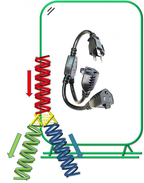
Researchers at Arizona State University, in collaboration with NYU and Duke University, have recently designed, created and tested a DNA circuit capable of splitting and combining current, much like an adapter that can connect multiple appliances to a wall outlet.
Graphic by Limin Xiang
Recently, researchers have found that DNA's remarkable properties of self-assembly and its ability to conduct electrical charge over considerable distance make it ideally suited for myriad applications, including tiny electronic circuits and computing devices, nanorobots and new advances in photonics.
Researchers at Arizona State University, in collaboration with NYU and Duke University, have recently designed, created and tested a DNA circuit capable of splitting and combining current, much like an adapter that can connect multiple appliances to a wall outlet.
Nongjian "N.J." Tao, a co-author of the new study, has been working on refining the ability of DNA to more stably and efficiently transport charge, an essential hurdle on the path to a new generation of biologically-based devices.
"The ability of DNA to transport electrical charge has been under investigation for some time," says Tao, who directs the Biodesign Center for Bioelectronics and Biosensors. "Splitting and recombining current is a basic property of conventional electronic circuits. We'd like to mimic this ability in DNA, but until now, this has been quite challenging."
Current splitting in DNA structures with three or more terminals is difficult as charge tends to rapidly dissipate at splitting junctions or convergence points. In the new study, a special form, known as G-quadruplex (G4) DNA is used to improve charge transport properties. As the name implies, G4 DNA is composed of four rather than two strands of DNA that are rich in the nucleotide guanine.
"DNA is capable of conducting charge, but to be useful for nanoelectronics, it must be able to direct charge along more than one path by splitting or combining it. We have solved this problem by using the guanine quadruplex (G4) in which a charge can arrive on a duplex on one side of this unit and go out either of two duplexes on the other side" says Peng Zhang, an assistant research professor of chemistry at Duke University and a co-author of the new study.
"This is the first step needed to transport charge through a branching structure made exclusively of DNA. It is likely that further steps will result in successful DNA-based nanoelectronics that include transistor-like devices in self-assembling 'pre-programmed' materials," Zhang says.
Along with Tao and Zheng, the research team consisted of Tao's ASU colleagues, Limin Xiang and Yueqi Li; Ruojie Sha and Nadrian C. Seeman of NYU; and Chaoren Liu, Alexander Balaeff, Yuqi Zhang and David N. Beratan of Duke University.
DNA is a highly attractive material for the design and creation of new nanoelectronics. The molecule's four nucleotide bases labelled A,T,C and G can be programmed to self-assemble into iconic double-helices, snapping together like matched puzzle pieces, A always bonding with T and C with G. A vast array of two-and three-dimensional DNA forms have been synthetically designed and built on these simple principles.
But the molecule can also assemble to form G4 DNA. Indeed, naturally-occurring guanine-rich quadruplex DNA serves a number of important physiological functions. Such DNA configurations occur at the ends of linear chromosomes, in structures known as telomeres, which play a critical role in the regulation of aging. DNA quadruplexes in telomeres have been shown to decrease the activity of telomerase-an enzyme responsible for telomere length and implicated in about 85 percent of all cancers. G4 quadruplexes are hence the drug target for important therapeutics.
In G4 structures, DNA takes the form of stacked guanine bases that form hydrogen bonds with their two immediate neighbors. The G4 structure at the heart of the new experiments, with its improved properties of charge transport, allowed researchers, for the first time, to design effective conducting pathways between the stacked G-quadruplex DNA and the double-stranded wires that form the terminals for either splitting or merging electrical current flow.
Earlier efforts to create such a Y-shaped electrical junction using only conventional double-stranded DNA had failed, due to the very poor charge transport properties inherent in the circuit's junction points. Using G4 DNA as a connector element in multi-ended DNA junctions was shown to dramatically improve charge transport through both three and four terminal DNA circuits.
The study directly measured conductance of charge through the G4-based nanostructure, using a device known as a scanning tunneling microscope or STM. The DNA molecule consisting of the G4 core with double-stranded wires forming the splitting terminals is chemically immobilized between a gold substrate and the gold tip of the STM device.
The tip of the STM is repeatedly brought in and out of contact with the molecule, breaking and reforming the junction while the current through each terminal is recorded. Thousands of traces were collected for each DNA candidate molecule. Using this break junction STM method allowed the researchers to design, measure and fine-tune a variety of prototype circuits for maximal charge transport properties.
"My role in this project was to measure the conductance outputs from the two DNA duplexes in our design," said Biodesign researcher Limin Xiang. "If you think about the power strip in your workplace, my task was to check whether each of the outlets is working properly. Surprisingly we found that the output currents from the two DNA duplexes are the same, with minimal energy loss. Our next step is to build more complicated DNA circuits by using this design as the basic element."
The study examined Y-shaped circuits that split the charge between three terminals (G4+3) as well as 4 terminal (G4+4) structures. Due to subtle distinctions in the charge transport properties of the two experimental circuits, the G4+4 motifs showed dramatically lower conductance values.
These results point to the G4+3 configuration as a more effective charge splitting and combining device. In this case, charge enters the junction from one terminal and exits through one of the other two terminals with almost equal efficiency.
The study marks an important first step in establishing G4 structures capable of efficiently carrying charge through three or more terminals, an essential requirement for control and electronic networking capabilities.
In addition to furnishing the growing field of DNA nanotechnology with new tools, the research may help illuminate Nature's methods of maintaining genetic integrity within cells and shed new light on myriad diseases linked with the breakdown of DNA error-correcting mechanisms.
